BACKGROUND: Many of us have heard the statement “the most important characteristic of a reliable solder connection is good wetting.” IPC J-STD-001 and IPC-A-610 include criteria for the degree of wetting or the percentage of area wetted. IPC J-STD-001 even includes one clause (4.18) that explains what constitutes acceptable wetting; however, it never explains what the mechanisms of wetting are or what is needed to achieve acceptable wetting.
The goal of this article is to explain what good wetting is and how to achieve it. We will provide examples of poor wetting and explain why it poses a risk to long-term reliability. To make this goal easier to achieve, we are going to explain the terms solderability, wetting and intermetallics, and why they are important to us as we strive to achieve the highest quality solder connections for our customers.
SOLDERABILITY
We start by discussing the term solderability. The solderability of a material is a measure of how easy or difficult it is to form a solder connection to that material. When trying to form a solder connection with wooden toothpicks

Figure 1. Poor solderability of wooden toothpicks

Figure 2. Good solderability of freshly tinned leads
(Figure 1), it is an example of poor solderability. Forming a solder connection with freshly tinned copper leads (Figure 2) is an example of good solderability. What this means is if you start with parts that have poor solderability, it will be very difficult to achieve acceptable wetting even if you have a great process. This also means that if you start with parts that have good solderability, it will make it much easier to achieve good wetting; however, a bad process can sabotage the good solderability and still result in poor wetting. In other words, poor solderability almost always results in poor wetting, but good solderability does not always lead to good wetting.
Now that we know what solderability is, we need a way to measure the solderability. There are both quantitative (objective properties) and qualitative (subjective properties) tests for solderability.
The most common qualitative test is what is known in the industry as the “dip and look” test. This test has been in use for decades. It was available in MIL-STD-202, Method 208, and then later as IPC J-STD-002, Test A. Although the “dip and look” test has very detailed procedures in an effort to improve consistency, the post-test evaluation is where it has opportunity for subjectivity. As a simplified example of the test, a component lead would be dipped in a solder bath and when removed it would be examined for the percentage of solder coverage. Solder coverage of 95 percent or greater in what would be the critical area would be considered passing.
 A very common quantitative solderability test is the wetting balance test (per IPC-J-STD002, 4.3) (Figure 3). The advantage of this test is that it provides objective, measureable values that can be used for comparison. The only important disadvantage is it is difficult to establish a universal pass/fail value because of the amount of variables involved in the manufacturing process.
  A part that might have great solderability for one manufacturer might exhibit poor solderability for another manufacturer as a result of their process differences. This test measures wetting force as a function of time. As the component lead is lowered to the surface of the solder bath, it encounters some initial resistance from the surface tension of the solder. Once wetting occurs, the initial resisting force is eliminated and a pulling force is exerted on the component lead. This is displayed as a two-axis curve (Figure 4) with force measured in the Y axis and time measured in the X axis. As long as the lead geometries are the same, it is possible test multiple components from different vendors and determine which one has the best solderability.

Figure 5. Contact angles are measured where the solder joins the other surface

Figure 6. Device with a convex fillet and a concave fillet. Both have acceptable contact angles
It is important to keep in mind that there are a lot of variables (solder alloy used, flux type, flux volume, ambient or inert atmosphere) in the soldering process. These variables will affect the minimum level of solderability that is necessary to achieve acceptable connections. If you have a forgiving process with a large process window, even marginal solderability may work.
WETTING
Now that we have discussed solderability, we move on to wetting. The IPC J-STD-001 document states that “the solder connection wetting angle shall not exceed 90°.” So what is this wetting angle that is also known as a dihedral angle?
The contact angle is measured where the solder fillet shape makes contact with the other metal, usually copper. We will look at this as the intersection of two planes (Figure 5). Do not confuse the fillet shape with the contact angle. You can have a concave fillet with good wetting, and a convex fillet with good wetting (Figure 6).

Figure 7. A very low contact angle indicating a very wettable surface
In Figure 7, there is a very low angle of approximately 7°. Low contact angles indicate the surface was easier to wet.

In Figure 8, we measure the contact angle at 45°. This surface was not as easy to wet as the previous example.

Figure 9. Maximum wetting angle that can be considered acceptable
In Figure 9, we have an angle of approximately 90°. This is the maximum acceptable angle and indicates that it was more difficult to get the solder to wet this surface.

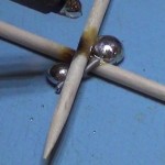
Figure 10. Solder will ball up on non-wettable surfaces with contact angles greater than 90°
Figure 10 has an angle of 148°. The solder is behaving as if the copper is a non-wettable surface, taking on a spherical shape. This far exceeds the 90° maximum.
Now that we know how to measure solder contact wetting angles, it is time to learn why contact angles that exceed 90° are not acceptable.

Figure 11. Stresses are very localized

Figure 12. Stresses are distributed over a large area
Once the finished electronic assemblies are put into service they are subjected to thermal and mechanical stresses. This is why we have bend radius requirements for leads, wires and cables. If a bend is too sharp (Figure 11) it tends to focus thermal and mechanical stresses in that location, which can reduce long-term reliability. Bends with a large bend radius (Figure 12) can distribute those stresses over a much larger area, which can improve long-term reliability.

Figure 13. Fractured solder connection
One of the biggest concerns is fractures and cracks that may occur in the solder connection (Figure 13). It is unusual to see a fracture formed anywhere except at some type of boundary or seam. Fractures are always looking for the path of least resistance and they need a starting point.

Figure 14. The birth of a fracture as a result of an excessive contact angle.
When a solder contact angle exceeds 90° it forms an interface that tends to focus stresses in the same way a cable with a tight bend radius does (Figure 14).
INTERMETALLICS

Figure 15 Required heat, metals, and flux
We have discussed solderability and wetting. Now it is time to see how wetting occurs.
We need three things for a good solder connection (Figure 15). Heat is required to melt the solder. We also need compatible metals. Finally we need flux to provide us with clean surfaces. Heat can be delivered by a soldering iron, a reflow oven, and other methods and equipment. Generally, metals compatibility is out of our control because it is determined by engineering. Solderable terminations may be copper with a plated finish. Flux is used to remove oxidation from the surfaces to be soldered. This allows the solder to make intimate contact with the plated finish.

Figure 16. This is an electroless nickel-immersion tin (ENIG) finish so the resulting intermetallics are nickel-tin
To understand wetting we need to understand the metals used in the soldering process. The metal of particular importance is Tin. Tin is used in both Sn63 solder and in the most common lead-free solders. Tin is a critical element of the soldering process because it loves to dissolve other metals and form molecular bonds that we call intermetallics. When the conditions are met, some of the tin will dissolve from the solder and together with the copper will form copper/tin molecules that are the intermetallics (Figure 16). As more solder is fed into the connection and the conditions are good, the solder will continue to wet over the intermetallic layer.

Figure 17. Solder can be removed easily from the glass surface
If we remove any of the three conditions we will have little to no wetting. If, for example, we have heat and a clean glass surface instead of a compatible metal, the solder can be removed easily (Figure 17). This is because no intermetallic formation would occur.

Figure 18. Solder fracture along the border of the intermetallics
To conclude we would like to make a quick comment about the love/hate relationship with intermetallics. Obviously, we need intermetallics or the solder would not adhere to the surface (just like our glass example). We do not want a lot of intermetallics because it has a coarse grain structure when compared to the copper or the solder. This coarse grain structure is the weakest part of the solder connection and when fractures occur they usually occur in or near the intermetallic layer (Figure 18).
SUMMARY
Now you should have a good grasp of what is acceptable wetting and what is not acceptable. Keep in mind that the J-STD-001 does specify what constitutes good wetting (contact angle not greater than 90°), but it usually does not require complete wetting of the entire connection area except for specific connection types.
Good luck and good wetting.
Acknowledgements:
Microsections, SEM Micrographs, Technical Guidance
Marietta Lemieux, STI Electronics, Inc., Manager Analytical Lab Services
To find out more about STI Electronics, please visit http://www.stielectronicsinc.com/


NEWSLETTER


Views


Skyscraper 1